DDR5 is the fifth era of Twofold Information Rate Simultaneous Unique Irregular Access Memory, also known as DDR5 SDRAM. Its improvement was started in 2017 by the business norms body JEDEC (Joint Electron Gadget Designing Gathering) with input from the main worldwide memory semiconductor and chipset engineering sellers, including Kingston. DDR5 is planned with new highlights for better execution, lower power and more vigorous information trustworthiness for the following 10 years of figuring. DDR5 appeared in 2021.


More noteworthy beginning pace execution
DDR5 debuts at 4800MT/s*, while DDR4 finishes out at 3200MT/s. This addresses a half expansion in transmission capacity. In rhythm with process stage discharges, DDR5 has arranged execution builds that will scale to 6400MT/s.
Decreased power/expanded productivity
At 1.1V, DDR5 consumes ~20% less power than DDR4 comparable parts at 1.2V. As well as preserving battery duration in workstations, it likewise enjoys a critical benefit for big business servers working nonstop.
PMIC
DDR5 modules highlight on-board Power The executives Coordinate Circuits (PMIC), which assist with managing the power expected by the different parts of the memory module (Measure, register, SPD center point, and so on). For server-class modules, the PMIC utilizes 12V; for PC-class modules, it utilizes 5V. This makes for better power conveyance contrasted with past ages, works on signal respectability and decreases clamor.
SPD center
DDR5 uses another gadget that coordinates the Sequential Presence Identify (SPD) EEPROM with extra center elements, oversees admittance to the outer regulator and decouples the memory load on the inner transport from outside.
Double 32-cycle subchannels
DDR5 parts the memory module into two free 32-cycle addressable subchannels to expand proficiency and lower the latencies of information gets to for the memory regulator. The information width of the DDR5 module is as yet 64-cycle. Be that as it may, separating it into two 32-digit addressable channels increments by and large execution. For server-class memory (RDIMMs), 8-pieces are added to each subchannel for ECC support for a sum of 40-bits per subchannel, or 80-bits per rank. Double position modules highlight four 32-bit subchannels.
Module key
The score in the focal point of the module behaves like a key, lining up with DDR5 attachments to forestall DDR4, DDR3 or other unsupported module types from being introduced. Not at all like DDR4, DDR5 module keys vary between module types: UDIMM and RDIMM
On-kick the bucket ECC
On-kick the bucket ECC (Blunder Rectification Code) is another element intended to address bit mistakes inside the Measure chip. As Measure chips expansion in thickness through contracting wafer lithography, the potential for information spillage increments. On-bite the dust ECC mitigates this gamble by revising blunders inside the chip, expanding dependability and decreasing deformity rates. This innovation can’t right mistakes beyond the chip or those that happen on the transport between the module and memory regulator housed inside the central processor. ECC-empowered processors for servers and workstations include the coding that can address single or multi-digit mistakes on the fly. Additional Measure bits should be accessible to permit this rectification to happen, as highlighted on ECC-class module types, for example, ECC unbuffered, enrolled and load diminished.
Extra temperature sensors
Server-class DDR5 RDIMMs and LRDIMMs add temperature sensors to the closures of the modules to screen warm circumstances across the length of the DIMM. This considers more exact control of framework cooling, rather than the choking of execution seen in DDR4 for high temperatures.
Expanded banks and burst length
DDR5 copies the banks from 16 to 32. This takes into consideration more pages to be open at an at once. The base burst length is additionally multiplied to 16, up from 8 for DDR4. This further develops information transport productivity, giving two times the information on the transport, and thusly decreases the quantity of peruses/writes to get to similar reserve information line.
Improved invigorates
DDR5 adds another order called SAME-BANK Invigorate, which permits a revive of only one bank for each bank bunch, versus all banks. When contrasted with DDR4, this order permits DDR5 to additionally develop execution and proficiency.
Choice Criticism Evening out (DFE)
DDR5 utilizes Choice Criticism Evening out (DFE) to give steady, dependable sign respectability on the module, which is expected for high data transfer capacity.
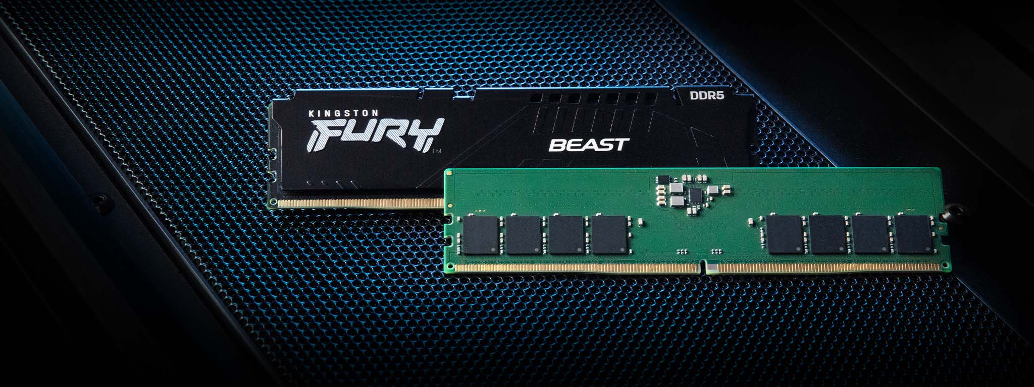
Structure factors
While the memory modules themselves seem like DDR4, there are massive changes that make them contrary with inheritance frameworks. The key area (score in the middle) moves to keep them from being introduced into contrary attachments.
DIMM: 288 pins
SODIMM: 262 pins
Enlisted DIMMs
Load-decreased DIMMs
ECC unbuffered DIMMs
ECC unbuffered SODIMMs
Non-ECC unbuffered DIMMs
Non-ECC unbuffered SODIMMs
| Data rates (speed in MT/s) | 4000, 4400, 4800, 5200, 5600, 6000, 6400 MT/s |
| Monolithic DRAM densities (Gbit) | 8Gb, 16Gb, 24Gb, 32Gb, 48Gb, 64Gb |
| Package type and ballout (x4, x8 / x16) | BGA, 3DS TSV (78, 82 / 102) |
| Interface | |
|---|---|
| Voltage (VDD / VDDQ / VPP) | 1.1 / 1.1 / 1.8 V |
| Internal VREF | VREFDQ, VREFCA, VREFCS |
| Command/Address | POD (Pseudo Open Drain) |
| Equalisation | DFE (Dynamic Feedback Equalisation) |
| Burst length | BL16 / BC8 / BL32 (optional) |
| Core architecture | |
| Number of banks | 32 banks (8 bank groups) 8 BG x 4 banks (16-64Gb x4/x8) 8 BG x 2 banks (8Gb x4/x8) 16 banks (4 bank groups) 4 BG x 4 banks (16-64Gb x16) 4 BG x 2 banks (8Gb x16) |
| Page size (x4 / x8 / x16) | 1KB / 1KB / 2KB |
| Prefetch | 16n |
| DCA (Duty Cycle Adjustment) | DQS and DQ |
| Internal DS delay monitoring | DS interval oscillator |
| ODECC (On-Die ECC) | 128b+8b SEC error check and scrub |
| CRC (Cyclic Redundancy Check) | Read/Write |
| ODT (On-Die Termination) | DS, DS, DM, CA bus |
| MIR (“Mirror” pin) | Yes |
| Bus inversion | Command/address inversion (CAI) |
| CA training, CS training | CA training, CS training |
| Write levelling training modes | Improved |
| Read training patterns | Dedicated MRs for user-defined serial, clock and LFSR-generated training patterns |
| Mode registers | Up to 256 x 8 bits |
| PRECHARGE commands | All bank, per bank and same bank |
| REFRESH commands | All bank and same bank |
| Loopback mode | Yes |